Moore’s Law Is Dying.
2 nanometers. That is approximately 10 to 20 atoms wide, depending on the element. TSMC began volume production of 2nm chips in Q4 2025, ramping hard through 2026, with initial yield rates of approximately 70%.
Last verified Also on Medium

On this page
2 nanometers. That is approximately 10 to 20 atoms wide, depending on the element. TSMC began volume production of 2nm chips in Q4 2025, ramping hard through 2026, with initial yield rates of approximately 70%. The entire production capacity of TSMC’s first 2 dedicated 2nm fabs is booked through the end of the year. Apple holds more than half of that initial allocation, with its A20 processor for the next iPhone generation, its M6 chip for Mac, and the Vision Pro R2 wearable chip all queued for the N2 node. AMD, Qualcomm, Nvidia, and MediaTek are directly behind.
TSMC’s 2nm capacity is expanding fast, from 40,000 wafers per month at the end of 2025 to a target of 100,000 per month in 2026 and 200,000 per month by 2027. The node uses gate-all-around nanosheet transistors combined with backside power delivery, a combination that resets the power-performance curve in ways that FinFET scaling could not. This is genuinely impressive engineering.
Then, in the space of about a week in late June 2026, 3 separate organisations announced things that collectively suggest TSMC’s achievement, extraordinary as it is, may be the last act of one era rather than the opening of another. Huawei, IBM, and OpenAI each announced something different, from 3 different directions, and each one is saying the same underlying thing: shrinking transistors sideways is no longer the primary lever of progress.
What is striking is that none of them sound alarmed. They sound like engineers who have already figured out what comes next.
Before getting into the 3 announcements, you need to understand why Moore’s Law is actually running out, because the explanation in most coverage is wrong. The problem is not that transistors are getting too small to shrink further. The problem is where the energy goes.
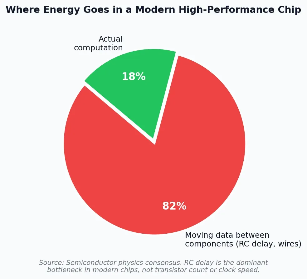
More than 80% of the energy consumed by a modern high-performance chip does not go toward computation. It goes toward moving information between components inside the chip. This is the number that the product launch presentations never mention, because it is not a marketable feature. It is a fundamental constraint.
Think of a chip as a city. Transistors are the buildings where the actual work happens. The microscopic metal wires connecting them are roads. A modern chip has more than 20 layers of those roads stacked on top of each other. Every signal traveling through those wires runs into 2 forces working against it: the resistance of the metal, and what engineers call parasitic capacitance, an invisible charge effect along the wire that has to cycle with every piece of information that passes through. The longer the path, the worse both effects compound. Engineers call this the RC delay, and it is the actual bottleneck in modern chips, not transistor size.
Processor clock speeds have stagnated for 15 years not because transistors stopped shrinking but because the paths between them are still too long.
This is why processor clock speeds have stagnated for roughly 15 years despite transistor counts continuing to grow. You can pack more transistors onto the chip, but if the signals still have to travel long distances to reach each other, you gain density without gaining speed. The solution that Huawei, IBM, and OpenAI are each converging on is the same one: stop building wider and start building upward, compressing the distances signals need to travel.
Huawei’s 7-Year Detour That Might Redefine the Industry
In June 2026, at the International Circuit and Systems Symposium in Shanghai, He Tingbo, president of HiSilicon, Huawei’s chip design arm, presented a new architectural approach called Logic Folding. This was He Tingbo’s first major public appearance in years, during a period when Huawei has been largely cut off from the equipment that TSMC uses to make chips at advanced nodes. ASML’s EUV lithography machines, which cost hundreds of millions of dollars each and require export licences that US sanctions have blocked, are essential for patterning features below roughly 7nm with a single exposure pass. SMIC, Huawei’s foundry partner, has been compensating by making multiple passes over the same pattern: 3, 4, sometimes 5 successive exposures where TSMC does it in 1. This works up to a point. Every additional pass adds defects and manufacturing complexity.
That ceiling forced a genuinely important question. Is horizontal transistor shrinkage actually the right direction? Huawei’s answer is no, and Logic Folding is their alternative. The concept takes a circuit that normally spreads flat across silicon and folds it vertically, like folding a piece of paper in half. Stack the logic layers on top of each other and components that were separated by millimetres of horizontal distance are now separated by microns of vertical distance. The signal path collapses. The RC delay that was limiting performance collapses with it.
Huawei claims 55% higher transistor density and 41% better energy efficiency without a single EUV machine. If the thermal challenge is solved, sanctions may have accidentally accelerated the next era of chip design.
Alongside Logic Folding, Huawei introduced what they call the Tau law, a new framework for measuring chip progress not by transistor width but by signal propagation time across the system. Progress measured in time rather than in nanometres. The claimed performance numbers are striking: up to 55% higher transistor density and 41% better energy efficiency without a single EUV machine in the manufacturing chain. Their upcoming Kirin 2026 processor, the first commercial chip using this architecture and expected in late 2026, is reportedly targeting 238 million transistors per square millimetre. That figure would be comparable to TSMC’s first-generation 3nm node, achieved through vertical integration rather than lateral shrinkage.
The legitimate engineering challenge embedded in this claim is worth naming. Communication between 2 stacked active logic layers at the required speeds depends on millions of tiny copper connections called bonding interconnects. Huawei says they are targeting a bonding pitch of 1.5 microns, compared to roughly 9 microns at the current industry best. That is 6 times tighter than anything that exists today in production. Managing the heat generated by 2 stacked active logic layers inside a smartphone form factor, without the liquid cooling that server racks can use, is the other constraint that needs to be solved.
The historical precedent for constraints producing innovation is strong enough that this does not feel like a reason to dismiss the approach. When the US cut GPS signals to Europe during the Kosovo conflict in 1999, Europe built the Galileo satellite navigation system. When the 1973 oil embargo hit Japan, Japan became the world leader in fuel efficiency. Huawei’s CEO has said publicly that the sanctions forced a direction Huawei would not have taken voluntarily.
IBM’s 0.7 Nanometre Chip and What the Number Actually Means
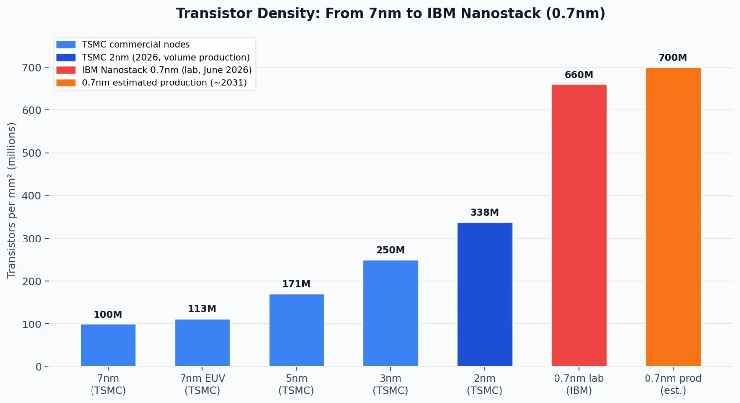
On June 25, 2026, IBM announced the world’s first sub-1 nanometre semiconductor technology, presented at the VLSI 2026 Symposium in Kyoto. The node is called 0.7nm, or 7 angstroms. 7 angstroms is approximately 7 atoms wide.
Before going further, the naming caveat is worth stating clearly. A node name in semiconductors is no longer a physical measurement. The Next Web’s analysis of the announcement notes this explicitly: a 0.7nm node does not mean any feature on the chip is 0.7 nanometres across. It is a generation label. What the number signals is relative progress against prior generations, and on that basis the IBM announcement is significant.
The architecture IBM unveiled is called Nanostack. Instead of continuing to shrink transistors laterally, Nanostack builds them in 2 stacked vertical layers on the same wafer, one directly on top of the other, fabricated sequentially. IBM demonstrated a working CMOS inverter, confirming the structure can be physically built and can switch. IBM’s press release confirmed approximately 100 billion transistors on a fingernail-sized die, roughly twice the density of IBM’s own 2nm chip from 2021, with up to 50% higher performance or 70% better energy efficiency compared to that 2nm predecessor.
IBM’s Nanostack delivered 40% SRAM scaling in a single step solving a problem the industry had quietly given up on since TSMC’s 3nm node.
The SRAM result may be the most practically important finding for AI specifically. SRAM is the ultra-fast on-chip memory that lives inside a processor and serves as the buffer for the most computationally intense operations. It had essentially stopped shrinking at TSMC’s 3nm node. IBM’s Nanostack delivers 40% SRAM scaling in a single step. IBM projects Nanostack-based AI accelerators could reach 7,000 TOPS, compared to approximately 1,500 TOPS in current leading-edge chips, and could cut large language model training time from roughly 3 months to 2 weeks.
The honest context is that this is a laboratory result, not a product. IBM does not manufacture logic chips at commercial volume. It licenses its architectures to partners. The 2nm chip IBM announced in 2021 has only recently approached broad commercial deployment, 5 years after its announcement. Nanostack production is probably 5 years from commercial silicon. But laboratory demonstrations in this industry are the map, and this map extends below 1 nanometre for the first time with validated hardware.
IBM Research director Jay Gambetta framed it directly: “With our new nanostack architecture, we’re not just making smaller transistors, we’re reinventing how chips are built to deliver dramatically more power and energy efficiency.”
OpenAI’s Jalapeño: The Chip That AI Designed in 9 Months
On June 24, 1 day before IBM’s announcement, OpenAI and Broadcom unveiled Jalapeño, OpenAI’s first custom-built inference processor. Bloomberg reported that Broadcom CEO Hock Tan confirmed a 50% reduction in cost per inference compared to current Nvidia GPU-based inference, with first deployments planned before the end of 2026.
Jalapeño went from initial concept to manufacturing tape-out in 9 months. A design of this complexity typically takes 2 to 3 years. AI compressed the timeline by a factor of 3 by helping design the chip it will run on.
What is genuinely novel about Jalapeño is not just the performance specification. It is the design timeline. A chip of this complexity would typically require 2 to 3 years from initial design to manufacturing tape-out. Jalapeño went from initial concept to tape-out in 9 months. The acceleration came from using OpenAI’s own models to assist with significant portions of the design and optimisation process. AI accelerated the design of the chip that AI will run on.
The loop this creates is worth pausing on. AI designs a chip. The chip runs AI more efficiently. That AI helps design the next chip more quickly. Each generation compresses the timeline of the next. If the 50% inference cost reduction holds in production, and if the design cycle continues to compress, the economics of running large language models at scale change faster than the conventional semiconductor roadmap would suggest.
OpenAI is also not alone in this direction. Google has been designing its own TPU chips for over a decade and is now on its 7th generation. Amazon has its Trainium and Inferentia lines. Microsoft is developing its Maia series. Meta has released details of its MTIA inference chip. The hyperscalers collectively represent an enormous shift of AI compute demand away from commodity GPU hardware toward purpose-built silicon.
What All 3 Are Actually Saying
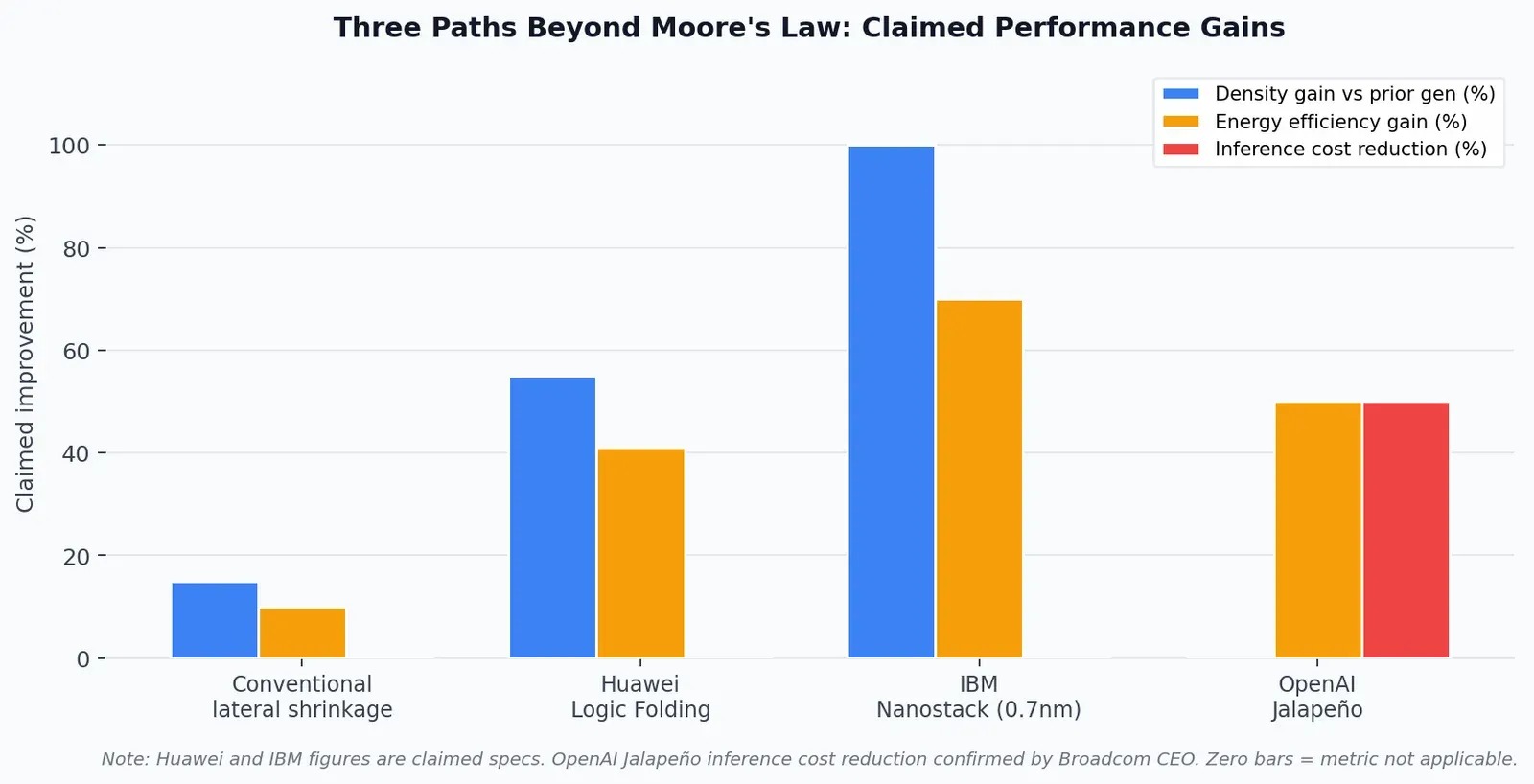
Set the 3 announcements side by side and the common thread is unmistakable. Huawei is folding logic vertically to collapse signal paths without EUV access. IBM is stacking transistors at the transistor level to break below 1 nanometre. OpenAI is designing custom chips optimised for the specific matrix operations that large language models perform, compressing the design cycle with the same intelligence the chip will eventually run.
None of them is competing on transistor width. All of them are competing on signal travel time, on vertical density, on design intelligence, and on system-level integration. The era where progress was reliably measured in nanometres of width is closing.
The broader industry is converging on the same direction. AMD has been stacking memory on processors for 3 years with its 3D V-Cache technology. Intel is routing power delivery through the back of the wafer on its latest process designs. TSMC is preparing its own version of vertical integration for the nodes after N2.
For AI specifically, this matters in a direct economic way. The cost of running a large language model is determined almost entirely by GPU compute efficiency. If Jalapeño delivers on its 50% inference cost reduction when deployed before year-end, the economics of AI inference shift immediately. If IBM’s Nanostack architecture makes it to production in 5 years, the projected AI accelerator performance of 7,000 TOPS would represent roughly a 5x improvement over current leading hardware. If Huawei’s Logic Folding proves its thermal management thesis, it demonstrates that the path to competitive chip performance no longer requires access to the world’s most expensive lithography equipment.
The companies that understand what is happening are designing the full stack: the silicon, the memory layout, the packaging, and the power architecture together rather than separately. The advantage in the next decade of AI will not belong to whoever has the largest model. It will belong to whoever can run intelligence most efficiently at scale, and that is now a hardware problem as much as a software one.
These 3 announcements arrived in the same week by coincidence of timing. That coincidence makes them more interesting, not less. When Huawei, IBM, and OpenAI each independently pivot toward the same architectural direction at roughly the same moment, it is a reasonable signal that the direction is correct.
The physics that limited horizontal transistor scaling has been known for years. The engineering responses to those limits have been arriving throughout this decade. Last week, 3 of them arrived together and pointed in the same direction clearly enough that paying attention seemed warranted.
Sources
- IBM Official Press Release: IBM Debuts World’s First Sub-1 Nanometer Chip Technology, June 25, 2026 –0.7nm Nanostack at VLSI 2026. 100B transistors, 50% performance or 70% energy efficiency vs 2nm, 40% SRAM scaling, Jay Gambetta quote.newsroom.ibm.com. Accessed 10 July 2026.
- Forbes: IBM Unveils World’s First Sub-1nm Chip, June 25, 2026 — Transistor-level vs package-level 3D stacking. Working CMOS inverter. Mixed channel materials per layer.forbes.com. Accessed 10 July 2026.
- The Next Web: IBM says it has built the first sub-1nm chip technology — Node naming caveat: 0.7nm is a generation label not a physical measurement.thenextweb.com. Accessed 10 July 2026.
- Let’s Data Science: IBM debuts 0.7nm Nanostack with nearly 100B transistors — 7,000 TOPS AI accelerator projection vs 1,500 TOPS current. Training time 3 months to 2 weeks. 40% SRAM scaling at VLSI 2026.letsdatascience.com. Accessed 10 July 2026.
- Interesting Engineering: IBM’s 0.7nm Nanostack, June 2026 –50% performance or 70% energy efficiency vs 2nm. Commercial adoption within 5 years.interestingengineering.com. Accessed 10 July 2026.
- SemiWiki: TSMC’s 2nm Chips Results, January 2026 — Apple accounting for more than half of initial 2026 2nm capacity. Qualcomm, MediaTek, AMD, Nvidia confirmed customers.semiwiki.com. Accessed 10 July 2026.
- Dr Robert Castellano: TSMC’s 2nm Era Technology Leadership, August 2025 –40,000 to 200,000 wafer per month ramp timeline. GAA nanosheet transistors with backside power delivery.drrobertcastellano.substack.com. Accessed 10 July 2026.
- New Market Pitch: TSMC Update, June 2026 — TSMC 72.3% vs Samsung 6.5% foundry share Q1 2026. AMD EPYC Venice N2 confirmed.newmarketpitch.com. Accessed 10 July 2026.
- Apple Insider: Nvidia Squeezing Out Apple for TSMC Capacity, January 2026 — HPC at 57% of TSMC revenue by Q3 2025.appleinsider.com. Accessed 10 July 2026.
- Wikipedia: Extreme Ultraviolet Lithography — ASML’s monopoly on EUV machines. China prototype EUV development December 2025.en.wikipedia.org. Accessed 10 July 2026.
- heqingele.com : TSMC 2nm Yield Rates and Mass Production Status 2026 — Volume production Q4 2025. 70% initial yield rates. 100,000+ wafers per month target.heqingele.com. Accessed 10 July 2026.
Related stories

Infrastructure
A Gas Pipeline Is Breaking America’s $500 Billion AI Bet
Oracle just moved to defer rent on its flagship Stargate data center before it opens. The reason is not chips or compute, it is a permit fight over a pipe, and the borrowed money behind the project means one delay travels everywhere.

AI & GPU compute
Nvidia’s Board Backed Jensen Huang on Sunday. By Thursday He Was Gone.
Four days after Nvidia’s board said it had confidence in its CEO, Jensen Huang resigned. A short seller had flagged the Megaspeed connection 6 months earlier, and most of the story rests on anonymous US officials, so I separate the filed facts from the allegations.
AI & GPU compute
25 GPUs for Local AI Ranked by Value, and a 2018 Server Card Takes Top Tier
A November 2026 price snapshot grades 25 cards on dollars per gigabyte and dollars per token per second. The AMD Instinct MI50 and a used RTX 3060 take S tier, the RTX 5080 lands in F, and memory decides almost every grade.